2.2. Getting Started Creating Verilog Cores
This guide will show you how to get started creating verilog projects that are easy to build, simulate and debug. Once your are done with a verilog core Ibuilder can incorporate the core into an FPGA image.
2.2.1. Prerequisits
The main Getting Started must be completed before following this guide.
2.2.2. Requirements
2.2.2.1. Scons
Scons or Software Construction Tool is a build tool similar to Make but instead of using the Make syntax it uses Python based syntax
Installation on Ubuntu
Within a terminal enter:
sudo apt-get install scons
Installation on Windows
Download and install scons
2.2.2.2. Icarus Verilog and GTKWave
IVerilog is used to compile and simulate your verilog projects
GTKWave is a logic waveform visualizer
Installation on Ubuntu Within a terminal enter
sudo apt-get install verilog
sudo apt-get install gtkwave
Installation on Windows Download and install Icarus Verilog
2.2.3. First Nysa Verilog Core Project (CBuilder Project)
Although the tool will allow you to create a cbuilder project in any directory, it is good to put it in a place that the ibuilder tool can find it. The best place to put it is your nysa_base/user_cbuilder_projects directory, which is usually located at <home>/Projects/nysa_base on Ubuntu and C:\Users\<name>\Projects\nysa_base on Windows
Navigate to that directory:
cd ~/Projects/nysa_base/user_cbuilder_projects
Generate a slave project:
nysa generate-slave --major 0x0F wb_test_core
In a hurry? skip to What was generated?
2.2.3.1. generate-slave command explanation
The generate-slave command will create a verilog project with the name you specify. Here are the features of the command
$> nysa generate-slave --help
 usage: nysa generate-slave [-h] [--axi] [--major MAJOR] [--minor MINOR]
                            [-o OUTPUT]
                            name

 create a project to generate a nysa compatible core

 positional arguments:
   name                  Specify the name of the project file

 optional arguments:
   -h, --help            show this help message and exit
   --axi                 Set the bus type as AXI (Wishbone by default)
   --major MAJOR         Specify the slave identification number (hex), use
                         "nysa device" command to view a list of possible
                         device IDs
   --minor MINOR         Specify the sub ID number (hex), used to identify a
                         unique version of a device Example: a unique GPIO that
                         uses internal PWMs would have a unique Sub ID to
                         differentiate itself from other GPIO devices
   -o OUTPUT, --output OUTPUT
                         Specify a location for the generated project, defaults
                         to current directory

 Examples:

 Generate a Wishbone slave project in the current directory
     ID of 0x02 (GPIO)

         name generate-slave --major 2 <name>

 Generate a Wishbone slave project with a sub id number in a specified directory
     ID of 0x03 (UART)
     Sub ID of 0x02
     Output Directory: home/user/Projects/cbuilder_projects/project1

         name generate-slave --major 3 --minor 2 --output home/user/Projects/cbuilder_projects/project1 <name>

 Generate an Axi slave project (NOT IMPLEMENTED YET!)
     ID of 0x05 (SPI)

         name generate-slave --axi --major 5 <name>
The two things that should be specified when this command is used are the major and minor numbers. This is important because when you will eventually insert this core into an FPGA the host computer uses those two numbers to identify what the core is.
A list of available major numbers can be found using the nysa devices command:
$> nysa devices
Getting device list
Available Devices:
SDB                  0x01 : Self Describing Bus
GPIO                 0x02 : General Purpose Input Output
UART                 0x03 : Universal Asynchronous Receiver and Transmitter
I2C                  0x04 : Inter-IC Communication
SPI                  0x05 : Serial Peripheral Interface
Memory               0x06 : Generic Memory Device
Console              0x07 : Generic Output Console
FSMC                 0x08 : Flexible Static Memory Controller
LED                  0x09 : Light Emitting Diode
Buttons              0x0A : Buttons
Frame Buffer         0x0B : Generic Frame Buffer
I2S                  0x0C : Generic Inter IC Sound
Logic Analyzer       0x0D : Logic Analyzer
Camera               0x0E : Camera
Experiment           0x0F : Experiment
LCD                  0x10 : LCD Display
STEPPER              0x11 : Stepper Motor Controller
Clock Synth          0x12 : Clock Synthesizer
DMA                  0x13 : Direct Memory Access controller
Storage Manager      0x14 : Manage Storage Devices like SATA
DMA Reader           0x20 : A test core for DMA Reader
DMA Writer           0x21 : A test core for DMA Writer
Platform             0x22 : A Nysa Platform
For example in the wb_gpio core the major number is 0x02, and the minor number of 0x01 (Cospan Design’s version of the GPIO). This major and minor number help the software developers write drivers that will interact with your core within an actual FPGA.
If you don’t know what type of core you will be using you can enter 0x0F for Experimental. This value can easily be changed in the future.
2.2.4. What was generated?
The command generates a new directory with the name you specified, using the tree command in Ubuntu we can see the directory structure:
$> tree wb_test_core
wb_test_core
├── command_file.txt
├── README
├── rtl
│   └── wb_test_core.v
├── SConstruct
├── sim
│   ├── master_input_test_data.txt
│   ├── master_output_test_data.txt
│   ├── project_defines.v
│   └── tb_wishbone_master.v
└── site_scons
    └── utils.py

3 directories, 9 files
File meaning:
- README: file will also describe the directory contents
- command_file.txt: This is a list of files and commands that the build tool will read in. When adding new verilog files to your project don’t forget to tell the build tool about it in here.
- rtl/wb_test_core.v: This is the generated slave project
- SConstruct: used by the scons build tool to build the project, it’s very unlikely that this file should be edited
- site_scons/utils.py: used by the scons build tool to build the project: it’s very unlikely this file should be edited
- sim/tb_wishbone_master.v: A test bench that wraps around your core it also reads in the master_input_test_data.txt to stimulate your core. For simple cores this doesn’t need to be edited. When simulating more complicated cores that interface with an external device the simulated external device will be instantiated here.
- sim/master_input_test_data.txt: Write a list of commands that will be used to stimulate your core. This will be explained below.
- sim/master_output_test_data.txt: Output of a simulation session will output here as well as on the console.
- sim/project_defines.v: defines that will be available to the core in a real FPGA as well as a ‘SIM’ define to tell your core that we are in a simulation instead of an actual synthesis. It is safe to include this file within your core because the actual FPGA project will have a file with the same name that defines FPGA specific features such as the ‘clock rate’
The directory is a complete, ready to build, project. You can go into that directory and build the project by using the scons tool. move into the new directory and use scons.
scons
You will see this:
$> scons
scons: Reading SConscript files ...
Fixing verilog Paths...
scons: done reading SConscript files.
scons: Building targets ...
iverilog -odesign.sim -ctemp.txt
scons: done building targets.
What was built?
The output of this build is ready to simulate design.sim project. To simulate use the following command
scons sim
You will see this:
$> scons sim
scons: Reading SConscript files ...
Fixing verilog Paths...
scons: done reading SConscript files.
scons: Building targets ...
iverilog -odesign.sim -ctemp.txt
vvp -n design.sim
VCD info: dumpfile design.vcd opened for output.
ADDR: 00000000 user wrote 00000001
ADDR: 00000001 user wrote 0000000a
ADDR: 00000002 user wrote 0000000b
user read 00000000
user read 00000001
user read 00000002
user read 00000000
scons: done building targets.
The tool rebuilt the project then execute the simulation command vvp -n design.sim. The tb_wishbone_master.v file opened up the master_input_test_data.txt and executed the commands. This allows you to write test benches much faster than if you were to write raw verilog test benches.
2.2.4.1. master_input_test_data.txt
Here is the master_input_test_data.txt
#Command Format:
#[Data Count]:[Flags,Command]:[Periph Device, Address]:[Data(ignored for reads)]

#Ping
00000000:00000000:12345678:FEDCBA98

#Write one peice of data to the peripheral device 1, address 0, data 1
00000000:00000001:01000000:00000001

#Write three peices of data to the peripheral device 1, address 1, data A, B, C
00000003:00000001:01000001:0000000A
0000000B
0000000C
0000000D

#Read one peice of data from peripheal 1 address 0
00000000:00000002:01000000:00000000

#Read two peices of data from peripheral 1 address 1 (Data is a filler)
00000002:00000002:01000001:00000000

#Sleep
00000008

#Read one (1 and 0 are the same for data count) from peripheral 1 address 0
00000001:00000002:01000000:00000000
And line starting with ‘#’ are comments and will be ignored.
The command is broken down into four blocks
[Data Count]:[Flags,Command]:[Periph Device, Address]:[Data(ignored for reads)]
Data Count: Number of 32-bit words to read/write to the device NOTE: 0 and 1 are the same
- Commands:
Flags: These are modifiers to the commands, flags like auto increment the address
- Commands:
- 0: Ping
- 1: Write to the core
- 2: Read from the core
- Address: Only useful for both read and write but a value must be put in here for the ping command
- Peripheral address: This is the location of your core on the bus, normally enter 01 here because the core is the 2nd device on the bus.
- Address within your core: You access your cores using addresses, Address 0x000000 will address the first address within your core.
Data: Although this is only useful for write, a value must be put in for both read and ping, when more than one 32-bit value is written use the following lines to add more data
Note About Sleep: Sometimes you will want your core to process data for a number of clock cycles, adding a numeric value outside of a command will tell the simulator to let the core process for the specified number of cycles.
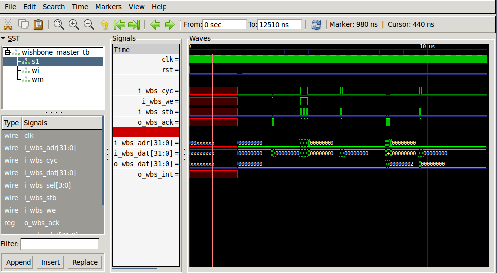
2.2.4.2. Waveforms
It helps a lot to visualize the waveforms. Use GTKWave to visualize the logic waveforms with the following command:
nysa wave
A new GTKWave window should open up in the background.
2.2.5. How to modify the core
The slave cores generate are simple wishbone slaves. It is designed to process commands that a wishbone master will send it. The entire set of commands are read and write.
2.2.5.1. Writing to the core
When we ran the simulation above we saw these lines towards the end:
...
ADDR: 00000000 user wrote 00000001
ADDR: 00000001 user wrote 0000000a
ADDR: 00000002 user wrote 0000000b
user read 00000000
user read 00000001
user read 00000002
user read 00000000
...
The first three lines:
...
ADDR: 00000000 user wrote 00000001
ADDR: 00000001 user wrote 0000000a
ADDR: 00000002 user wrote 0000000b
...
are result from a write that was initiated in the sim/master_input_test_data.txt
...
#Write one peice of data to the peripheral device 1, address 0, data 1
00000000:00000001:01000000:00000001

#Write three peices of data to the peripheral device 1, address 1, data A, B, C
00000003:00000001:01000001:0000000A
0000000B
0000000C
0000000D
...
Inside the wb_test_core/rtl/wb_test_core.v the core processed those commands here
...
//After the port declaration

//Local Parameters
localparam     ADDR_0  = 32'h00000000;
localparam     ADDR_1  = 32'h00000001;
localparam     ADDR_2  = 32'h00000002;

//Down a little more in the files
...
//write request
case (i_wbs_adr)
  ADDR_0: begin
    //writing something to address 0
    //do something

    //NOTE THE FOLLOWING LINE IS AN EXAMPLE
    //  THIS IS WHAT THE USER WILL READ FROM ADDRESS 0
    $display("ADDR: %h user wrote %h", i_wbs_adr, i_wbs_dat);
  end
  ADDR_1: begin
    //writing something to address 1
    //do something

    //NOTE THE FOLLOWING LINE IS AN EXAMPLE
    //  THIS IS WHAT THE USER WILL READ FROM ADDRESS 0
    $display("ADDR: %h user wrote %h", i_wbs_adr, i_wbs_dat);
  end
  ADDR_2: begin
    //writing something to address 3
    //do something

    //NOTE THE FOLLOWING LINE IS AN EXAMPLE
    //  THIS IS WHAT THE USER WILL READ FROM ADDRESS 0
    $display("ADDR: %h user wrote %h", i_wbs_adr, i_wbs_dat);
  end
  //add as many ADDR_X you need here
  default: begin
  end
endcase
...
Notice how 0x0000000C and 0x0000000D were ignored, this is because there is no case to process these commands
The first single write command wrote to address 0x00 of this 2nd slave (Slave ID 1) on the perpheral bus. inside wb_test_core.v the condition ADDR_0 was found and the simulation task $display("ADDR: %h user wrote %h", i_wbs_adr, i_wbs_dat); resulted in the values printed to the screen.
When writing a core that talks to a host computer, this is where the core would receive values from the host.
2.2.5.2. Reading from the core
The last four lines of the simulation file show four reads from the core
...
user read 00000000
user read 00000001
user read 00000002
user read 00000000
...
These commands were a result of the read requests issued within the master_input_test_data.txt file
#Read one peice of data from peripheal 1 address 0
00000000:00000002:01000000:00000000

#Read two peices of data from peripheral 1 address 1 (Data is a filler)
00000002:00000002:01000001:00000000

#Sleep
00000008

#Read one (1 and 0 are the same for data count) from peripheral 1 address 0
00000001:00000002:01000000:00000000
Here is where the reads occur within wb_test_core.v
//After the port declaration

//Local Parameters
localparam     ADDR_0  = 32'h00000000;
localparam     ADDR_1  = 32'h00000001;
localparam     ADDR_2  = 32'h00000002;

//Down a little more in the files
...
//read request
case (i_wbs_adr)
  ADDR_0: begin
    //reading something from address 0
    //NOTE THE FOLLOWING LINE IS AN EXAMPLE
    //  THIS IS WHAT THE USER WILL READ FROM ADDRESS 0
    $display("user read %h", ADDR_0);
    o_wbs_dat <= ADDR_0;
  end
  ADDR_1: begin
    //reading something from address 1
    //NOTE THE FOLLOWING LINE IS AN EXAMPLE
    //  THIS IS WHAT THE USER WILL READ FROM ADDRESS 0
    $display("user read %h", ADDR_1);
    o_wbs_dat <= ADDR_1;
  end
  ADDR_2: begin
    //reading soething from address 2
    //NOTE THE FOLLOWING LINE IS AN EXAMPLE
    //  THIS IS WHAT THE USER WILL READ FROM ADDRESS 0
    $display("user read %h", ADDR_2);
    o_wbs_dat <= ADDR_2;
  end
  //add as many ADDR_X you need here
  default: begin
  end
endcase
...
2.2.5.3. Modify the code
As a first edit we can make a 32-bit register that will store a value obtained when the user writes data to address 0x00 then return that same value to the user when they read address 0x00
on line 94 add the line:
reg [31:0] my_data;
it should look like this afterwards:
...
//Local Registers/Wires
reg     [31:0]  my_data;
//Submodules
//Asynchronous Logic
//Synchronous Logic

always @ (posedge clk) begin
  if (rst) begin
...
Initialize the register when a reset occurs at line
my_data <= 32'h0;
It should look like this afterwards:
...
always @ (posedge clk) begin
  if (rst) begin
    o_wbs_dat <= 32'h0;
    o_wbs_ack <= 0;
    o_wbs_int <= 0;
    my_data   <=  32'h0;
  end

  else begin
...
Put the data that is read into address 0 into the new register ‘my_data’
On line 126
...
my_data   <=  i_wbs_dat;
...
It should look like this afterwards:
...
case (i_wbs_adr)
  ADDR_0: begin
    //writing something to address 0
    //do something

    //NOTE THE FOLLOWING LINE IS AN EXAMPLE
    //  THIS IS WHAT THE USER WILL READ FROM ADDRESS 0
    $display("ADDR: %h user wrote %h", i_wbs_adr, i_wbs_dat);
    my_data   <=  i_wbs_dat;
  end
  ADDR_1: begin
...
Finally, return the data back to the host when the host requests data from address 0x00
On line 157 comment out o_wbs_dat <= ADDR_0; and replace it with the following:
...
o_wbs_dat <= my_data;
$display("user read from my_data: %h", my_data);
...
The code should look like this:
...
//read request
case (i_wbs_adr)
  ADDR_0: begin
    //reading something from address 0
    //NOTE THE FOLLOWING LINE IS AN EXAMPLE
    //  THIS IS WHAT THE USER WILL READ FROM ADDRESS 0
    $display("user read %h", ADDR_0);
    //o_wbs_dat <= ADDR_0;
    o_wbs_dat <= my_data;
    $display("user read from my_data: %h", my_data);
  end
  ADDR_1: begin
    //reading something from address 1
...
Now to test it out go to the console and enter the simulation command:
nysa sim
and you should see this
$> nysa sim

scons: Reading SConscript files ...
Fixing verilog Paths...
scons: done reading SConscript files.
scons: Building targets ...
iverilog -odesign.sim -ctemp.txt
vvp -n design.sim
VCD info: dumpfile design.vcd opened for output.
ADDR: 00000000 user wrote 00000001  <= Writing to my_data!
ADDR: 00000001 user wrote 0000000a
ADDR: 00000002 user wrote 0000000b
user read 00000000
user read from my_data: 00000001    <= Reading from my_data!
user read 00000001
user read 00000002
user read 00000000
user read from my_data: 00000001    <= Reading from my data again!!1
scons: done building targets.
If you want to change the data that is being written to the core modify master_input_test_data.txt on line 8
#Write one peice of data to the peripheral device 1, address 0, data 1
00000000:00000001:01000000:01234567
and the simulation output should change to:
scons: Reading SConscript files ...
Fixing verilog Paths...
scons: done reading SConscript files.
scons: Building targets ...
iverilog -odesign.sim -ctemp.txt
vvp -n design.sim
VCD info: dumpfile design.vcd opened for output.
ADDR: 00000000 user wrote 01234567
ADDR: 00000001 user wrote 0000000a
ADDR: 00000002 user wrote 0000000b
user read 00000000
user read from my_data: 01234567
user read 00000001
user read 00000002
user read 00000000
user read from my_data: 01234567
scons: done building targets.
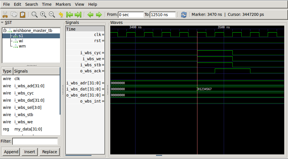
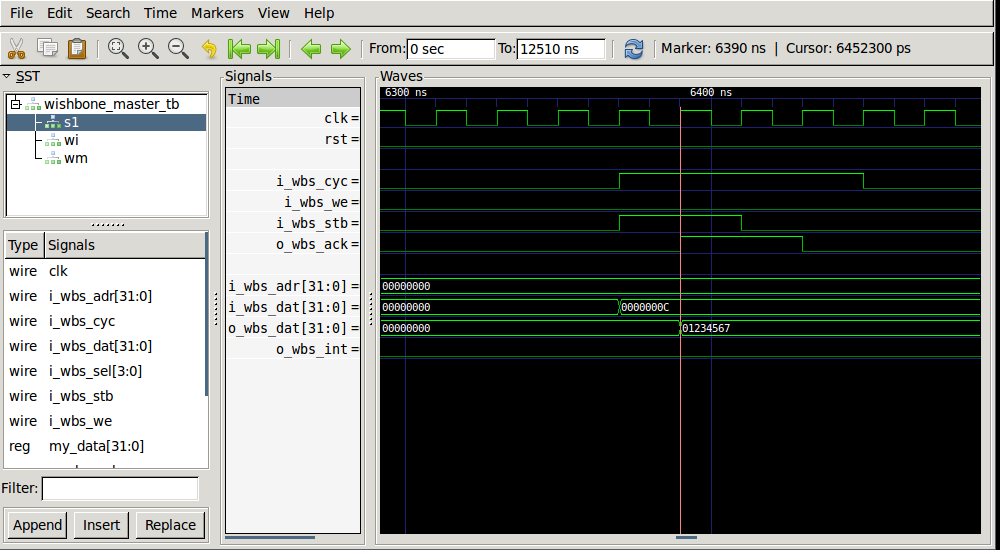
To visualize this we can open up a gtkwave session:
scons wave
and find the write sequence
and the read sequence
2.2.6. Conclusion
This verilog core is an introduction on how to get started developing cores for Nysa. This core can also be used in other wishbone based projects.
The great thing about this core is that it is also ready to be used within an FPGA project. in the getting started manual ‘Getting started with Ibuilder’ I’ll cover how to move this core to an actual FPGA image, then proceed to interfacing with that core using ‘Getting started with Nysa host’